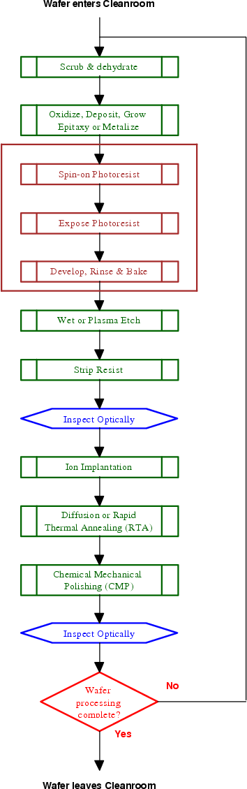
Wafer Fabrication Process Flow
An interesting variation of the standard silicon wafer is the silicon-on-insulator substrate. Using 193nm light sources brightfield inspection is the workhorse technology in the fab.

How A Semiconductor Wafer Is Made Usjc United Semiconductor Japan Co Ltd
The doped wafer formed will be the p-type substrate with the trivalent impurities.

. Smoothing things out the lapping and polishing process. It undergoes many microfabrication processes such as doping ion. Microfabrication is the process of fabricating miniature structures of micrometre scales and smaller.
A true prime wafer is a device quality wafer that any major fab could use for the latest technology semiconductor devices. At Intel we see the potential for using technology in the classroom to help students learn the skills necessary for. Sliced wafers need to be prepped before they are production-ready.
AMD VCE is an ASIC. Silicon wafers have been used abundantly in microelectronics and MEMS as a platform for fabrication. At present the largest silicon wafer is 300mm in diameter.
Excellent agreement is achieved between actual and modeled results. An application-specific integrated circuit ASIC ˈ eɪ s ɪ k is an integrated circuit IC chip customized for a particular use rather than intended for general-purpose use. The table below shows the process results obtained using the recipe listed above.
More than one hundred semiconductor dies are fabricated on a single wafer. Education technology EdTech is a powerful tool to connect students with learning opportunities. Advanced Micro Devices Inc.
Used to find defects during the transistor fabrication process brightfield collects light reflected from a defect. For example a chip designed to run in a digital voice recorder or a high-efficiency video codec eg. The Silicon dioxide layer or oxide layer is created on the surface that protects the substrate.
PUR-Therm was designed as a more efficient more precise mechanism for heating carrier gases and chamber process gases when compared to silicone wrap gas line heaters. Test wafers - A silicon wafer used in process monitoring or other testing. On this wafer we deposit repeating layers of silicon and silicon germanium a structure called a superlattice.
Historically the earliest microfabrication processes were used for integrated circuit fabrication also known as semiconductor manufacturing or semiconductor device fabricationIn the last two decades microelectromechanical systems MEMS microsystems. The largest wafer diameter used in semiconductor fabrication today is 12 inches or 300mm. PDMS is the most widely used silicon-based organic polymer as its versatility and properties lead to many applications.
Manufacturing Flow Chart of an Integrated Circuit 11 WAFER FABRICATION FRONT-END Identical integrated circuits called die are made on each wafer in a multi-step process. The recipe is the manufactures recommended process. In electronics a wafer also called a slice or substrate is a thin slice of semiconductor such as a crystalline silicon c-Si used for the fabrication of integrated circuits and in photovoltaics to manufacture solar cellsThe wafer serves as the substrate for microelectronic devices built in and upon the wafer.
On this wafer we deposit repeating layers of silicon and silicon germanium a structure called a superlattice. Building Skills for Innovation. Gases are isolated in a 25 63mm OD ultra-high purity seamless 316L seamless stainless steel flow tube with pre-installed industry-standard ultra-high purity VCR fittings.
Back EndBE Process Wafer Back Grinding The typical wafer supplied from wafer fab is 600 to 750μm thick. In the International System of Units the derived unit for voltage potential difference is named volt. It is particularly known for its unusual rheological or flow properties.
Also included in the table is the contact angle measured on a bare silicon wafer as a reference for the process. Each step adds a new layer to the wafer or modifies the existing one. In a fab chipmakers generally make use of several different types of wafer inspection tool technologies.
Voltage electric potential difference electric pressure or electric tension is the difference in electric potential between two points which in a static electric field is defined as the work needed per unit of charge to move a test charge between the two points. It uses a range of extreme ultraviolet EUV wavelengths roughly spanning a 2 FWHM bandwidth about 135 nm to produce a pattern by exposing reflective photomask to UV light. The silicon wafer is selected for doping p-type impurities on it.
Backfinish or wafer thinning before the wafer is scored and. To produce these wafers two sili- con wafers are bonded together by using silicon. These layers form the ele-ments of the individual electronic circuits.
It operates a 34 km-long X-ray laser which produces X-rays of unique quality for studies in physics chemistry the life sciences materials research and other disciplines. If defects are found the fabrication will be interrupted to remove the defects from the process and to make small changes in the fabrication conditions for correction purposes. The steps involved in the N-TUB fabrication process are as follows.
Use a large grit to coarsely grind the wafer and remove the bulk of the excess wafer thickness. European XFEL is an international non-profit company located in the Hamburg area in Germany. Semiconductor device fabrication is the process used to manufacture semiconductor devices typically integrated circuit.
A true prime wafer will be very smooth site inspected for flatness meeting a spec of at least 3um on a 20mm x 20mm site and defect free. Wafer thinned down to the required thickness 50um to 75um by abrasive grinding wheel. Use this area to filter your search results.
Each filter option allows for multiple selections. Polydimethylsiloxane PDMS also known as dimethylpolysiloxane or dimethicone belongs to a group of polymeric organosilicon compounds that are commonly referred to as silicones. The self-aligned 3D CMOS fabrication begins with a silicon wafer.
AMD is an American multinational semiconductor company based in Santa Clara California that develops computer processors and related technologies for business and consumer marketsWhile it initially manufactured its own processors the company later outsourced its manufacturing a practice known as going fabless after GlobalFoundries. Abrasive chemicals and machines polish the uneven surface of the wafer for a mirror-smooth finish. 1st step.
Regina Luttge in Microfabrication for Industrial Applications 2011. Suspensions of 2D hexagonal boron nitride show an anomalously large specific CottonMouton coefficient enabling the fabrication of a magnetically tuneable and stable birefringent optical device. Help ensure a laminar air flow to ensure that particles are immediately brought down to the floor and do not stay suspended in the air due to turbulence.
The self-aligned 3D CMOS fabrication begins with a silicon wafer. Extreme ultraviolet lithography also known as EUV or EUVL is an optical lithography technology used in steppers machines that make integrated circuits ICs for computers and other electronic devices. Application-specific standard product ASSP chips are intermediate between ASICs and.
Semiconductor manufacturers are. The Institute comprises 33 Full and 13 Associate Members with 12 Affiliate Members from departments within the University of Cape Town and 12 Adjunct Members based nationally or internationally.

Latest Vlsi Research Vlsi Updates Vlsi Training Study In Iits And Nits To Get A Good Job In Semic Semiconductor Semiconductor Manufacturing Diy Life Hacks

Basic Semiconductor Manufacturing Process
2 5 Fabrication

Improving The Sic Wafer Process Power Electronics News
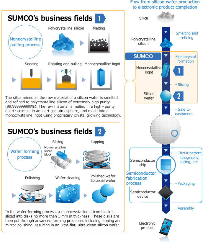
What Is Silicon Wafer Sumco Corporation
Die Prep Process Overview Wafer Dies Microelectronic Device Fabrication Packaging
0 Response to "Wafer Fabrication Process Flow"
Post a Comment